Jul 16, 2026Technology
DFM Analysis for PCBA | Prevent Manufacturing Defects Before Production
Discover how DFM and DFA analysis prevent PCB manufacturing defects, improve PCB assembly yield, shorten NPI cycles, and reduce production costs. Get a free DFM review before PCBA manufacturing.
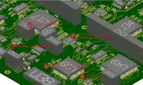
A failed PCBA rarely fails because of a single defective component. More often, the root cause was introduced weeks or even months earlier during the design stage.
Many engineering teams focus heavily on functionality, electrical performance, and cost optimization. Manufacturing feasibility is often treated as a later task. That assumption is expensive.
Once production begins, every design weakness becomes a manufacturing problem. Every manufacturing problem becomes a cost problem. Every unresolved quality issue eventually becomes a customer problem.
This is exactly why Design for Manufacturability (DFM) and Design for Assembly (DFA) have become essential steps before PCB fabrication and SMT assembly.
Common PCBA Problems That Damage Product Quality
Most PCBA failures can be grouped into four categories.
1. Design Defects
A PCB may pass electrical verification but still be difficult or impossible to manufacture efficiently.
Typical examples include:
- Insufficient solder mask clearance
- Trace spacing below fabrication capability
- Incorrect annular ring dimensions
- Components placed too close together
- Vias inside solder pads without proper treatment
- Missing fiducial marks
- Inadequate test point allocation
None of these issues prevent schematic completion.
Many of them do prevent stable mass production.
The cost difference between fixing these problems before manufacturing and after manufacturing can easily reach hundreds of times.
2. Assembly Problems
A PCB layout may satisfy electrical requirements while creating significant challenges during SMT assembly.
Common assembly issues include:
- Component shadowing during reflow
- Poor placement orientation
- Inconsistent polarity markings
- Large height differences causing placement instability
- Insufficient spacing for automated optical inspection (AOI)
- Difficult manual soldering areas
- Connector interference with production fixtures
These problems reduce production efficiency.
They also increase rework rates, labor costs, and manufacturing variability.
3. Quality Defects
Many field failures originate from design decisions rather than factory mistakes.
Examples include:
- Tombstoning
- Solder bridges
- Cold solder joints
- Insufficient solder fillets
- Excessive thermal stress
- PCB warpage
- Copper imbalance
- Moisture-sensitive component damage
The factory can only manufacture the board according to the provided data.
If the design itself introduces process instability, quality problems become unavoidable.
4. Responsibility and Cost Risks
When failures occur, determining responsibility becomes difficult.
The designer may blame manufacturing.
The factory may blame the PCB supplier.
The customer only sees one fact.
The product failed.
Warranty costs increase.
Project schedules slip.
Customer confidence declines.
Reputation suffers long after the technical issue has been corrected.
DFM and DFA Identify Problems Before They Become Production Losses
DFM is not simply a checklist.
It is a systematic engineering review that evaluates whether a design matches real manufacturing capability.
DFA extends this concept by ensuring that assembly processes remain stable, repeatable, and cost-effective.
Modern DFM analysis evaluates hundreds of manufacturing rules automatically, including:
- Minimum trace width and spacing
- Hole-to-copper clearance
- Solder mask opening
- Pad geometry
- Component spacing
- Thermal relief design
- Copper balance
- Panelization suitability
- Fiducial placement
- Stencil opening optimization
- SMT process compatibility
- Wave soldering restrictions
- AOI accessibility
- ICT testability
Instead of waiting for engineering questions after production starts, potential risks are identified immediately.
This changes the entire product development process.
Problems become engineering decisions rather than manufacturing emergencies.
DFM&DFA can Predict Manufacturing Problems Before the First Prototype
Traditional prototype development often follows a costly pattern.
Design.
Build.
Discover problems.
Modify.
Build again.
Repeat.
Every design iteration consumes engineering resources, purchasing time, fabrication capacity, and assembly scheduling.
DFM interrupts this cycle.
Potential manufacturing conflicts are identified before Gerber files enter production.
Component placement can be optimized.
Fabrication tolerances can be adjusted.
Assembly accessibility can be improved.
The first prototype becomes significantly closer to the final production version.
That translates directly into fewer engineering change orders (ECOs), fewer prototype revisions, and lower development costs.
DFM&DFA can Improve Product Reliability Instead of Simply Passing Functional Tests
Passing electrical testing does not guarantee long-term reliability.
Products experience thermal cycling.
Mechanical vibration.
Humidity.
Continuous power loading.
Transportation stress.
Design decisions directly influence how well a PCBA survives these conditions.
DFM reviews examine factors such as thermal distribution, copper balancing, solder joint reliability, component spacing, and mechanical support.
Small layout improvements often eliminate failure mechanisms that would otherwise appear months after deployment.
Reliability begins with design discipline, not warranty repair.
DFM Analysis can Shorten the Entire NPI Cycle
New Product Introduction (NPI) is usually delayed by repeated engineering corrections rather than fabrication speed.
Every unresolved manufacturing issue creates additional communication between design engineers, purchasing teams, PCB suppliers, and assembly factories.
Production schedules become unpredictable.
Material deliveries must be rescheduled.
Assembly slots are missed.
Product launch dates move further away.
A complete DFM review removes much of this uncertainty before production starts.
Engineering questions decrease.
Manufacturing approvals become faster.
Prototype success rates improve.
Mass production begins with greater confidence.
For companies operating under aggressive launch schedules, shortening even one prototype iteration can save several weeks.
Free DFM Review Before Manufacturing
Every PCB design contains assumptions.
Some are correct.
Some become expensive after production starts.
A professional DFM review exposes those risks while changes are still inexpensive.
Our engineering team provides a comprehensive DFM analysis before PCB fabrication and PCBA assembly.
The review covers manufacturability, assembly feasibility, process compatibility, and potential reliability risks.
You receive practical engineering feedback instead of generic design comments.
No obligation.
No hidden fees.
Finding one critical issue before production is far less expensive than correcting hundreds of assembled boards afterward.
If your PCB design is preparing for prototype or mass production, send us your Gerber files and BOM. Our engineers will perform a free DFM review and help identify manufacturing risks before they become production losses.