
Technology
HDI PCB Explained: What It Is, When You Need It, and How It's Made
Learn what HDI PCBs are, how microvias and buildup layers enable smaller, faster electronics, when your design needs HDI, and what drives the cost. Includes practical design and manufacturing guidance
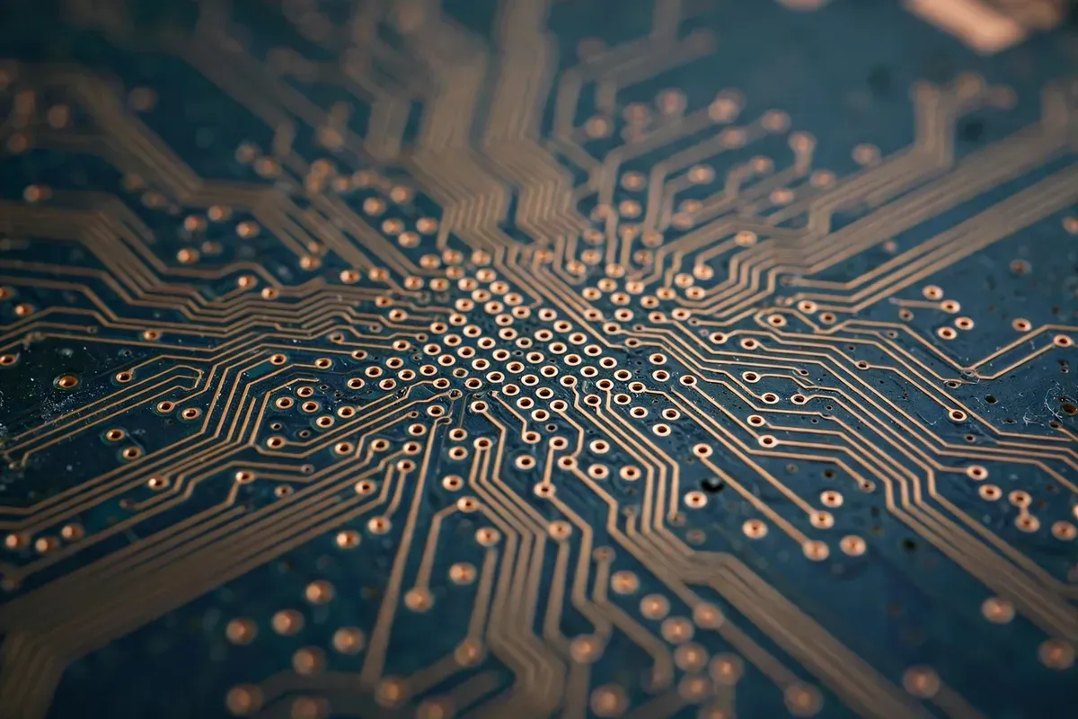
Your smartphone does more than the desktop computer from ten years ago, and it fits in your pocket. That progress was not driven by chips alone. The printed circuit board inside had to change just as radically.
A standard multilayer PCB reaches its limit quickly when a design combines fine-pitch components, high pin counts, and tight board space. Traces run out of room. Vias consume the space that routing needs. The board either grows larger or the design becomes unroutable.
High-Density Interconnect (HDI) PCB technology solves this problem. It packs more wiring into less area, shortens signal paths, and makes compact, high-performance electronics possible. This guide explains what HDI is, how it is made, when your design needs it, and what it costs.
What Is an HDI PCB?
An HDI PCB is a printed circuit board built with significantly higher wiring density per unit area than a conventional multilayer board. It achieves this with three key features:
- Microvias: very small vias, typically 0.15 mm (6 mil) in diameter or less, drilled by laser rather than mechanically.
- Blind and buried vias: vias that connect only selected layers instead of passing through the entire board.
- Via-in-pad: vias placed directly in component pads, freeing routing space on the surface.
HDI boards are manufactured with build-up layers: thin dielectric and copper layers laminated sequentially onto a central core. Each build-up cycle adds one layer per side, and microvias connect the new layer to the one below it.
The result is a board that routes far more connections in the same footprint, or the same connections in a much smaller footprint.
HDI vs. Standard Multilayer PCB
- Wiring density: microvias and via-in-pad free up routing channels that through-hole vias would block.
- Size and weight: the same circuit fits on a smaller, lighter board.
- Signal integrity: shorter traces and smaller vias reduce inductance and improve high-speed performance.
- Layer count: a complex design may need fewer layers in HDI than in standard multilayer construction.
- Cost: HDI costs more per board, because sequential lamination and laser drilling add process steps.
HDI is not better in every situation. It is better when density, size, or signal performance is the limiting factor.
HDI Stackup Types
1+N+1
One build-up layer on each side of the core. The simplest and most economical HDI structure. Suitable for designs that need a moderate density increase.
2+N+2
Two build-up layers on each side. Supports denser routing and finer-pitch components such as large BGAs.
Any-Layer HDI (ELIC)
Microvias on every layer, with connections possible between any two adjacent layers. Maximum routing freedom, and the highest manufacturing complexity and cost. Reserved for the most demanding designs, such as flagship smartphones.
Choosing a stackup is a trade-off between routing freedom and manufacturing cost. Most designs do not need any-layer HDI.
How HDI PCBs Are Manufactured
HDI manufacturing adds several steps to the standard PCB process:
- Core fabrication: the inner core is produced like a conventional multilayer board.
- Sequential lamination: build-up layers are laminated onto the core, one cycle at a time.
- Laser drilling: microvias are drilled with a laser, typically by UV or CO2 laser depending on the material.
- Metallization and plating: microvias are plated to create reliable electrical connections between layers.
- Via filling and capping: via-in-pad structures are filled and plated flat so components can be mounted directly on top.
- Fine-line imaging and etching: trace widths and spaces are typically finer than on standard boards.
- Testing: automated optical inspection (AOI), X-ray inspection of hidden vias, and electrical testing verify each board.
Each lamination cycle adds time and cost, which is why layer count is the main cost driver in HDI.
Key Design Considerations
Microvia aspect ratio
A laser microvia plates reliably when its depth is close to its diameter, roughly a 1:1 aspect ratio. Deeper, narrower vias risk incomplete plating and become a reliability concern.
Stacked vs. staggered microvias
Microvias on consecutive layers can be stacked directly on top of each other or staggered (offset). Stacked microvias save space but demand filled and capped construction. Staggered microvias are more forgiving and usually cost less.
Via-in-pad
Placing vias in pads frees significant routing space, but the vias must be filled and plated flat (VIPPO) or solder will wick into the hole during assembly and create weak joints.
Material selection
Standard FR-4 works for many HDI designs. High-speed designs, such as 5G modules and high-frequency radar boards, usually need high-Tg or low-loss laminates to control signal loss and heat.
Thermal management
Denser boards concentrate more heat in less area. Copper balance, thermal vias, and careful component placement matter more in HDI than in standard designs.
DFM review
HDI leaves less margin for error than standard PCB fabrication. A DFM review before production catches stackup, via, and spacing problems while changes are still inexpensive.
When Do You Actually Need HDI?
HDI is the right choice when:
- Fine-pitch BGAs or high pin-count components leave no room for fan-out routing
- The board must fit a fixed, compact enclosure (wearables, handheld medical devices)
- High-speed signals need shorter paths and controlled impedance
- Weight matters, as in drones, aerospace, and portable equipment
Typical applications include smartphones, tablets, wearable devices, medical electronics, automotive driver-assistance systems, lidar modules, 5G communication modules, and aerospace electronics.
HDI is not always necessary. If a standard multilayer board routes comfortably within your size and cost targets, HDI adds expense without benefit. The decision should follow the design's density requirements, not the technology trend.
What Drives HDI Cost?
- Number of build-up layers: each lamination cycle adds a full process loop.
- Microvia count and type: stacked and filled microvias cost more than staggered ones.
- Layer count overall: more layers mean more material and more testing.
- Material choice: low-loss and high-Tg laminates cost more than standard FR-4.
- Board size and volume: larger panels and higher volumes spread the fixed setup cost.
- Testing requirements: X-ray and advanced electrical testing add cost but are often essential for reliability.
Getting an accurate quote requires Gerber files and a clear stackup. Ballpark pricing without design data is rarely reliable.
Common HDI Design Mistakes
- Stacking microvias on every layer without considering reliability and cost
- Exceeding the aspect ratio that plating can handle reliably
- Forgetting to specify filled and capped vias for via-in-pad designs
- Using standard materials for high-frequency applications
- Routing high-speed signals without impedance control
- Skipping DFM review and discovering problems at the prototype stage
Most of these mistakes are inexpensive to fix during design and expensive to fix after fabrication.
Get Your HDI Design Reviewed Before Fabrication
HDI rewards careful design and punishes assumptions. A stackup that looks correct on screen can still hide manufacturing risks: an unplatable microvia, a thermal imbalance, or a via structure the assembly process cannot handle.
Our engineering team provides a free DFM review before PCB fabrication and PCBA assembly. The review covers stackup feasibility, microvia design, manufacturability, and assembly risks, with practical feedback you can act on.
If your design uses HDI, fine-pitch components, or dense routing, send us your Gerber files and BOM. We will review the design and help identify risks before they become production losses.