
Technology
Rigid-Flex PCB Design: Rules, Benefits, and Common Mistakes
Learn how to design rigid-flex PCBs: bend radius, keep-out zones, stiffeners, stackup and materials, plus the benefits over rigid boards and connectors.
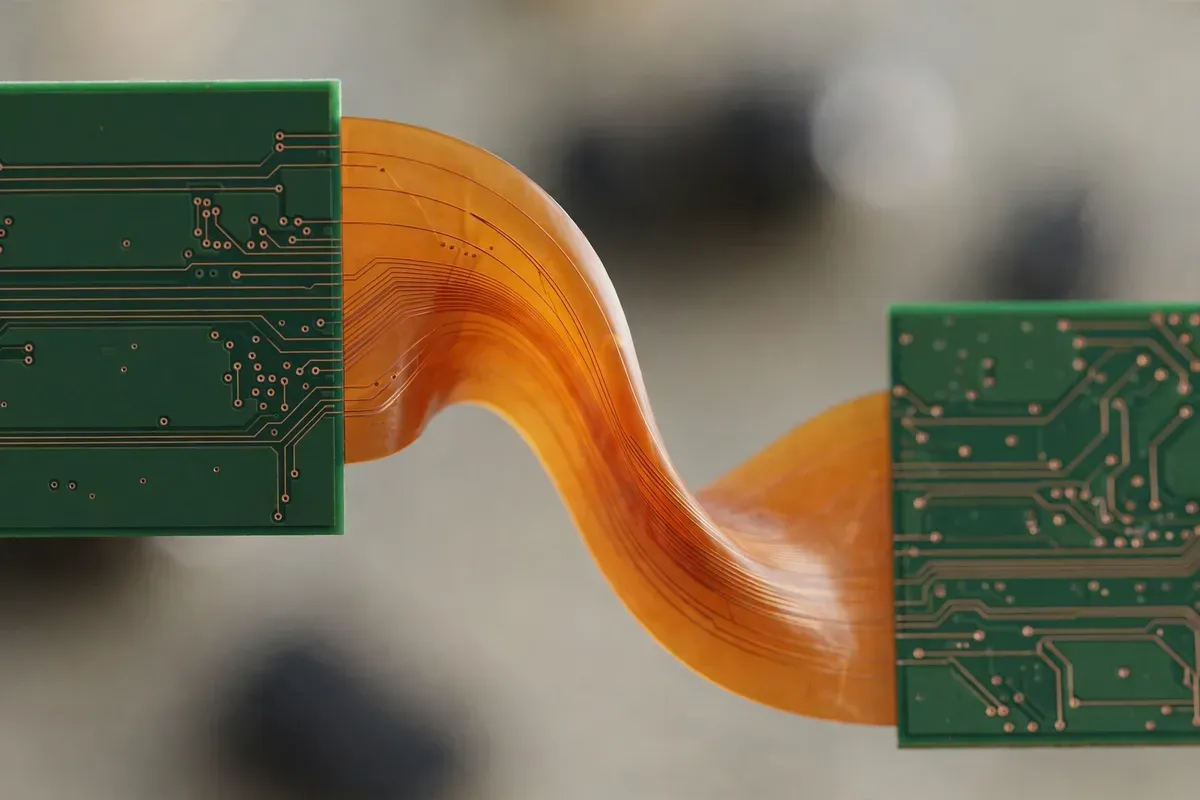
Some products cannot be built on a flat board. A wearable sensor wraps around a wrist. A camera module bends around a lens barrel. The circuit board must fit a three-dimensional shape, not the other way around.
The traditional solution is to split the circuit across several rigid boards and connect them with cables and connectors. It works, but every connector is a potential failure point, and every cable adds weight, assembly time, and cost.
A rigid-flex PCB takes a different approach. It combines rigid and flexible sections in a single board, so the circuit bends where it needs to bend and stays rigid where components must be mounted. This guide covers how rigid-flex boards work, the design rules that keep them reliable, and the mistakes to avoid.
What Is a Rigid-Flex PCB?
A rigid-flex PCB is one board that contains both rigid and flexible sections. The flexible layers, usually polyimide, run through the entire board. Rigid sections are formed by laminating additional FR-4 layers onto the flex layers.
The result is one board that folds into its final shape, with no cables or connectors between sections. Connections between rigid areas travel through the flex layers themselves.
Rigid-flex boards are used in two main ways:
- Flex-to-install: bent once during assembly and stays in that shape for the life of the product.
- Dynamic flex: bends repeatedly during use, as in folding devices or moving sensor heads.
Why Choose Rigid-Flex Over Rigid Boards and Connectors
- Reliability: fewer interconnects mean fewer failure points. Connector contacts and cable solder joints are among the most common sources of field failures, and rigid-flex eliminates them between sections.
- Space and weight: no connectors, no cables, no extra housing space for mating parts. The board folds into the available space instead of requiring room for connections.
- Simpler assembly: one board to assemble instead of several boards plus cables. Fewer parts to source, fewer steps on the production line, and fewer opportunities for assembly errors.
Rigid-flex is not the cheapest option per board. The savings come from the total product: fewer parts, simpler assembly, and lower field failure rates.
Key Design Rules
Rigid-flex design follows the same electrical rules as rigid PCB design, plus a set of mechanical rules that protect the flexible sections.
Bend radius
Every flex section has a minimum bend radius. Bend it tighter and copper traces crack, usually after the product has shipped.
A common rule of thumb for a static bend is a radius of at least six times the total thickness of the flex section. Multilayer flex sections need more, often ten times the thickness. Dynamic flexing needs a much larger radius, and as few layers as possible.
Keep-out zones in bend areas
The bend area is the most stressed part of the board. Nothing rigid belongs there.
Keep components, vias, and stiffeners out of the bend area, and leave a clear margin between the bend and the nearest via or component. A via in a bend area is a crack waiting to happen.
Traces should cross the bend line at right angles, not run parallel to it. Use curved traces instead of sharp corners in bend areas.
Stiffeners
Stiffeners are extra layers of FR-4 or polyimide bonded to the flex section where local rigidity is needed: under connectors, under components, or where the board is screwed to a housing.
A stiffener also adds thickness, which matters for connectors that require a specific board thickness, such as ZIF connectors. Plan stiffener locations early.
Stackup and layer planning
Flex layers run through the whole board, including the rigid sections. Rigid sections add FR-4 prepreg and core layers on top of the flex layers.
Keep the stackup symmetrical around the center of the board. An asymmetric stackup warps during lamination and soldering.
Use as few flex layers as the design allows. Each extra flex layer makes the bend section thicker and harder to bend reliably.
Material selection
Polyimide is the standard base material for flex sections. It tolerates soldering temperatures, resists chemicals, and survives repeated bending well.
Adhesiveless laminates are preferred for fine-pitch and high-reliability designs. They are thinner, handle heat better, and avoid an adhesive layer that can weaken with thermal cycling.
Flex areas are protected with coverlay, a polyimide film laminated over the traces, instead of liquid solder mask. Plan coverlay openings around the bend area, not across it.
Typical Applications
- Medical devices: hearing aids, implantable devices, and handheld diagnostic instruments, where small size and reliability are critical.
- Aerospace and defense: avionics, satellites, and radar systems, where weight savings and vibration resistance matter.
- Wearables and consumer electronics: smartwatches, fitness bands, and camera modules.
- Automotive: driver-assistance cameras, lidar modules, and dashboard electronics that must fit curved housings.
These industries also demand certified manufacturing. Our production is certified to IATF16949, ISO13485, ISO9001 and ISO14001, with US UL certification.
Manufacturing Considerations
Flex sections are fragile before assembly, so panels often include support rails and breakaway tabs.
Testing also differs. Electrical testing must verify the flex sections, and some designs need a bend test after assembly.
Lead times are longer than for standard rigid boards, so plan the schedule accordingly and avoid late design changes.
What Drives Rigid-Flex Cost?
- Layer count: more rigid and flex layers mean more material, more lamination cycles, and more processing cost.
- Material choice: polyimide and adhesiveless laminates cost more than standard FR-4.
- Yield: rigid-flex has more process steps than rigid PCB, and each step affects yield.
- Testing: bend testing, X-ray, and full electrical testing add cost but are often essential for reliability.
An accurate quote requires Gerber files, a stackup drawing, and the bend-area requirements. Pricing without that information is rarely reliable.
Common Rigid-Flex Design Mistakes
- Bending the flex section tighter than the minimum bend radius
- Placing vias or components in the bend area
- Running traces parallel to the bend line
- Designing an asymmetric stackup that warps during lamination
- Forgetting stiffeners under connectors mounted on flex sections
- Skipping DFM review and finding mechanical problems at the prototype stage
Most of these mistakes are inexpensive to fix during design and expensive to fix after fabrication.
Get Your Rigid-Flex Design Reviewed Before Fabrication
Rigid-flex rewards careful design and punishes assumptions. A bend radius that looks fine on screen can hide cracked traces.
Our engineering team provides a free DFM review before PCB fabrication and PCBA assembly. The review covers stackup feasibility, bend-area rules, manufacturability, and assembly risks.
If your design uses rigid-flex or tight three-dimensional packaging, send us your Gerber files and BOM. We will review the design and help identify risks before they become production losses.