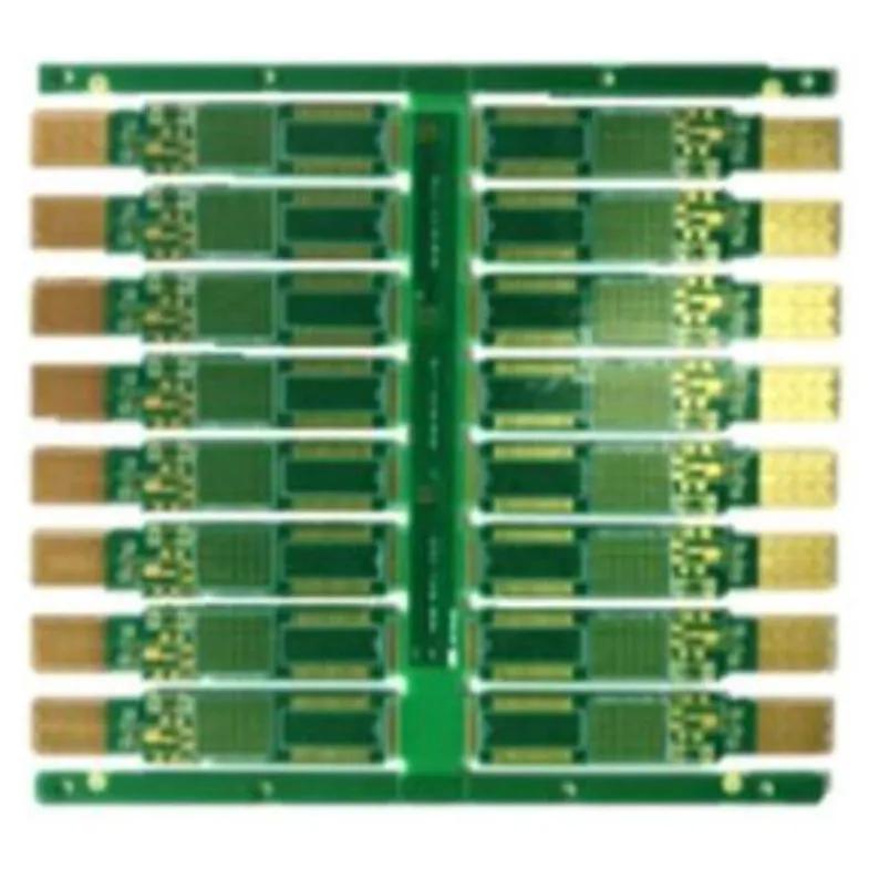
Telecommunications PCBA
Optical module (100G transmission signal) 8-layer HDI2 Segmented Golden Finger PCB
Application: Optical module (100G transmission signal) Layers: 8 L Features: HDI2 Segmented Golden Finger
Application: Optical module (100G transmission signal) Layers: 8 L Features: HDI2 Segmented Golden Finger
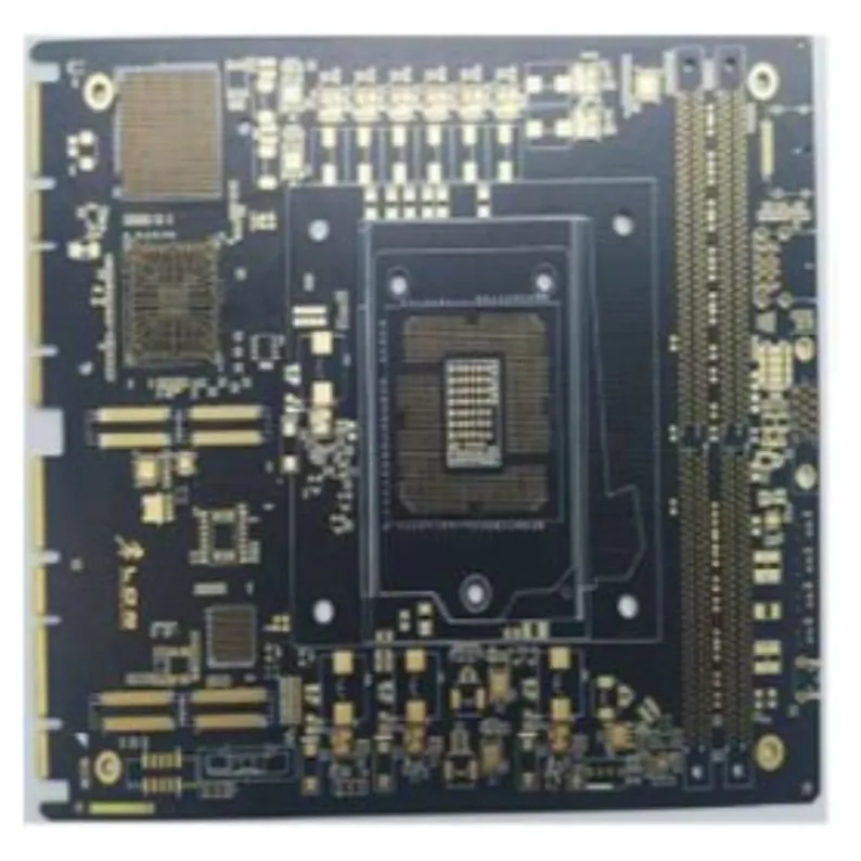
Application: Communication network card (40G Ethernet network) Layers: 12 L Features: 6 back-drilling operations
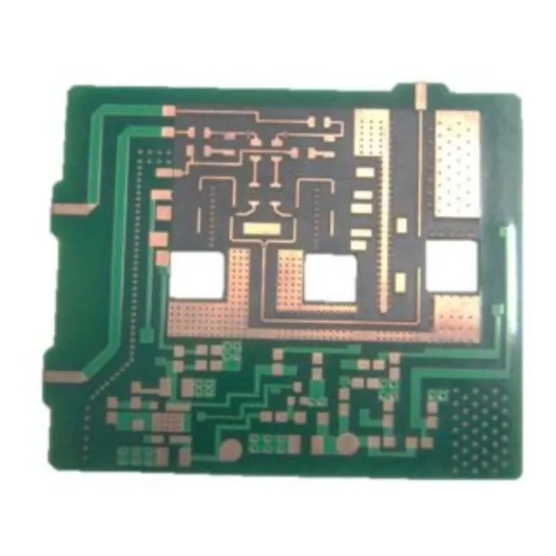
Application: Radar Layers: 4L Features: RT5880 Local Mixed Pressure
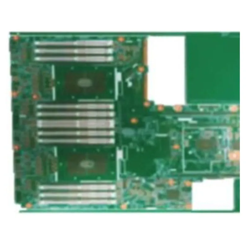
Application: server motherboard Layers: 12 L Features: thickness to diameter rate 10 :1
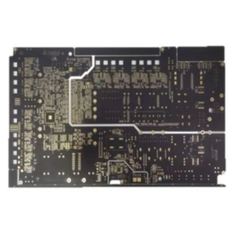
Application: charging pile Layers: 8 L Features: 2 oz thick copper
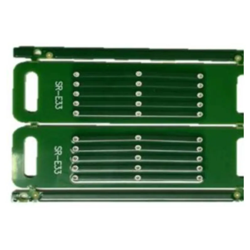
Application: generator brush Layers: 2 L Features: 7 oz thick copper
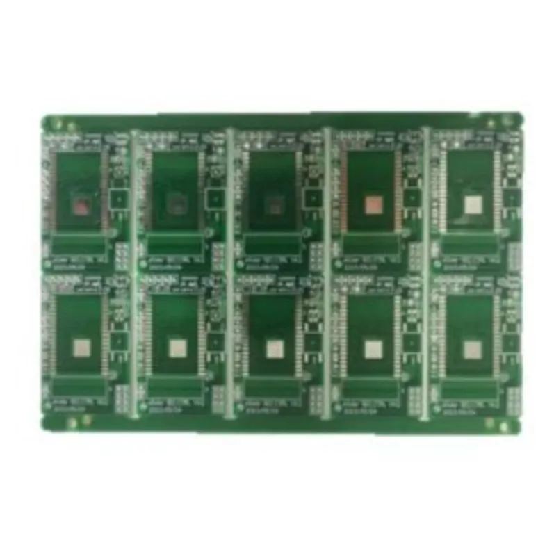
Application: Solar inverter Layers: 4 L Features: Crimping hole
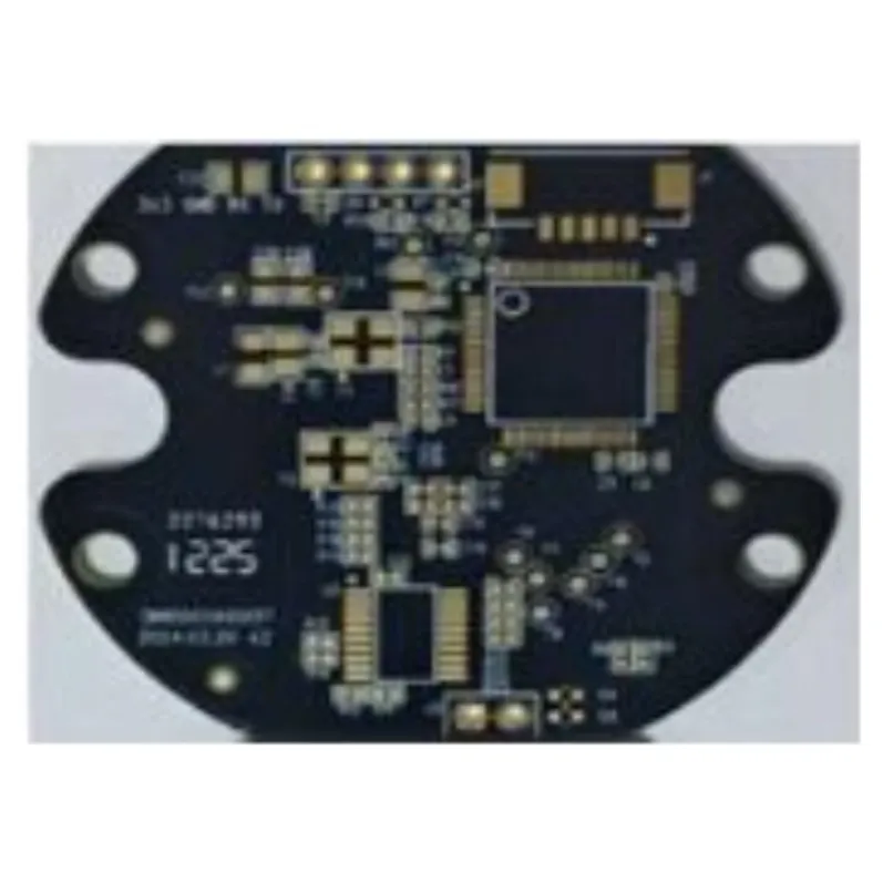
Application: Radar ranging sensor Layers: 4L Features:Through -hole
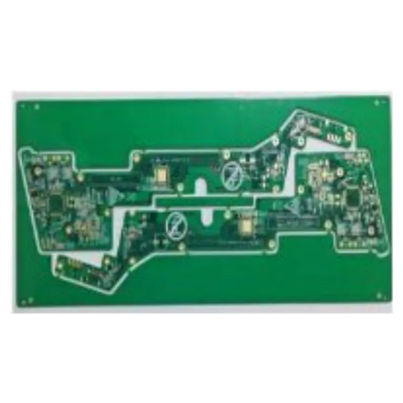
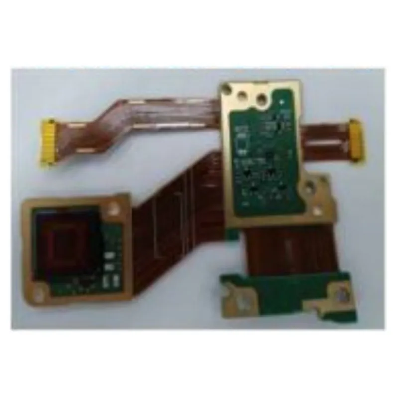
Application: Lidar Layers: 8L Features: 2nd-order HDI rigid-flex PCB
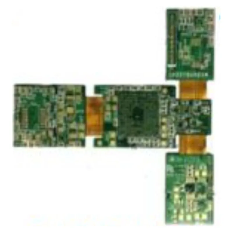
Application: Image processing Layers: 6L Features:rigid-flex PCB
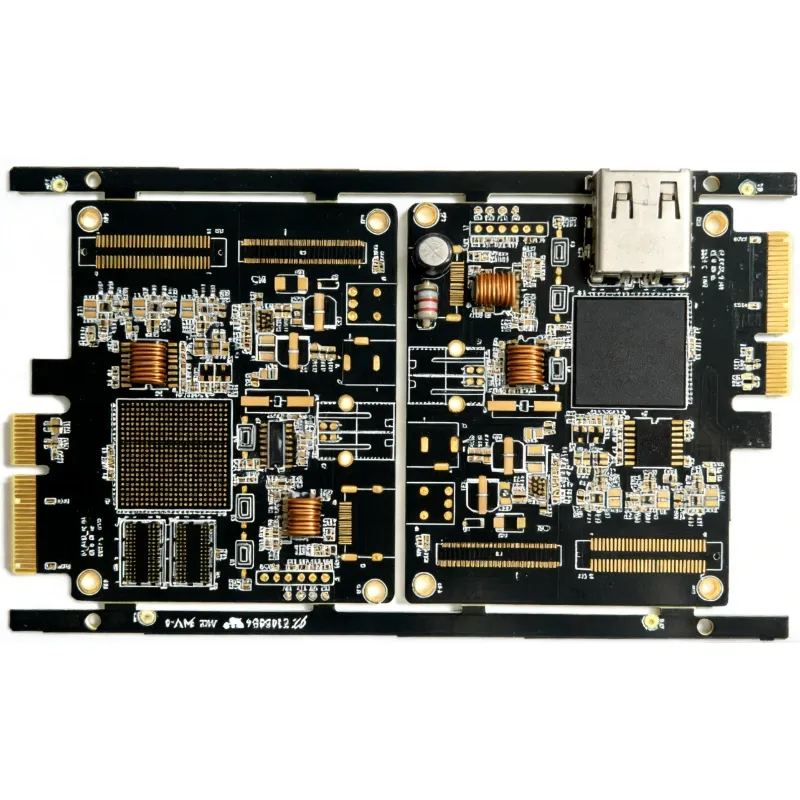
PCBA is fundamental in communication products for signal processing and data transmission. In routers and switches, it manages high-speed data packets for network traffic. In base stations, PCBA processes radio frequencies (RF) to enable 5G connectivity. It is used in fiber optic transceivers to convert electrical to optical signals. For satellites and smartphones, compact, high-frequency PCBAs ensure reliable wireless communication with minimal signal loss.